| |
Carrier mobility is one of the most important
properties in semiconductor devices, such as high electron mobility
transistor (HEMT) and field-effect transistor (FET), both of which are
capable for realizing terahertz (1012 Hz) ultra-high-speed
operation in telecommunication and optical memory. The carrier mobility
is determined by µ = eτ/m*, where e
denotes
electron
charge, τ is the carrier relaxation time introduced in the
relaxation time approximation, and µ represents
electron effective mass in n-type semiconductors. Here, the carrier
relaxation time τ includes all scattering processes, such as
electron-hole scattering, electron-phonon scattering (Frohlich and
deformation potentials), and scattering by defects and disorders. In
general, the time scale of τ is less than a few hundred
femtoseconds. While the carrier mobility has recently been obtained by
using THz time-domain spectroscopy with the fit by Drude
function, the accessible range of the carrier density was
limited to lower density than an order of 1016 cm-3,
due to
non-Drude behavior originating from nonthermal carrier distribution at
the high carrier density region.
In doped semiconductors, such as n-type
GaAs, it is well known that the plasmon and the longitudinal optical
(LO) phonon form coupled modes through Coulomb interactions, and the
frequencies of the LO phonon-plasmon coupled (LOPC) modes depend on the
carrier density Ne through the relation of the
plasma frequency. Using Raman spectroscopy Nakashima and Harima have
developed characterization of carrier mobility in SiC. They observed
plasmon-like LOPC modes in frequency domain and fit the spectra with
the line profile determined by frequency-dependent amplitude and
dielectric function. As the results of the fitting, they obtained
bandwidth of the plasmon-like LOPC mode, and put it into the formula
µ = e/m*γ, where γ is a damping rate
of plasmon. The derived carrier mobility matched very well to that
obtained by Hall measurements. Although Raman spectroscopy is a
promising tool to estimate carrier mobility without any mechanical
contact onto a sample, one need fitting of the line shape using a
number of equations.
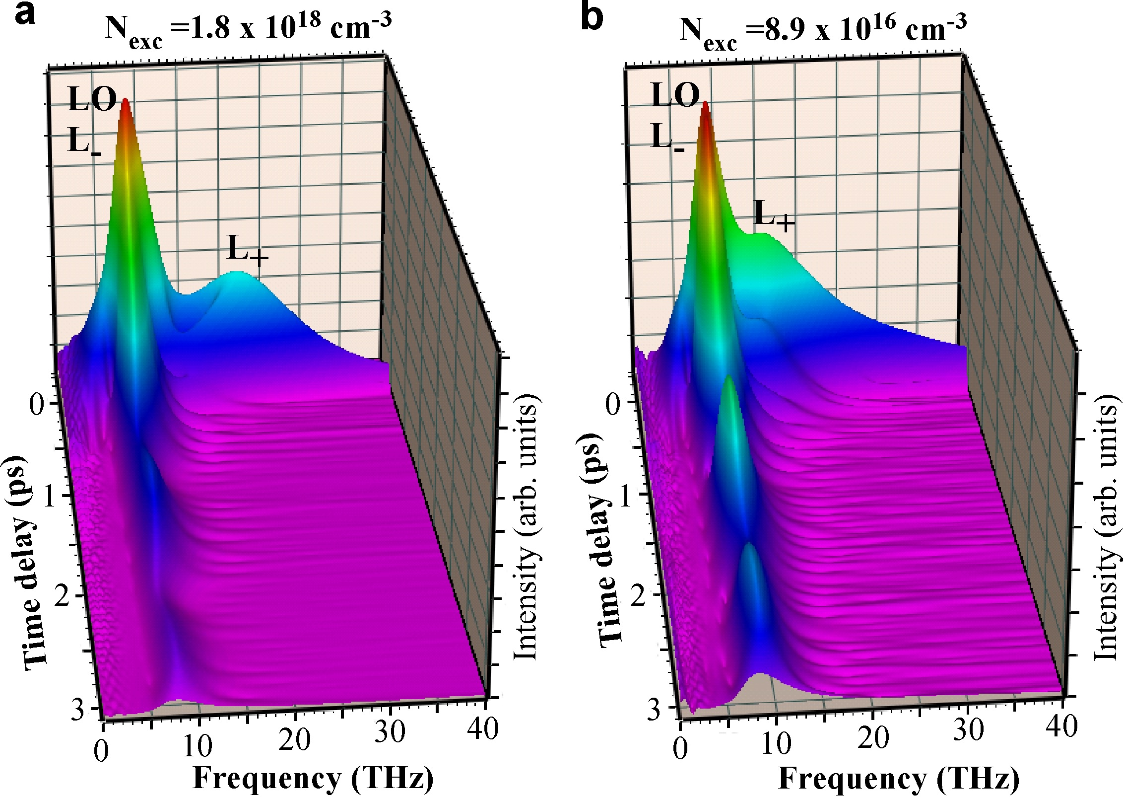
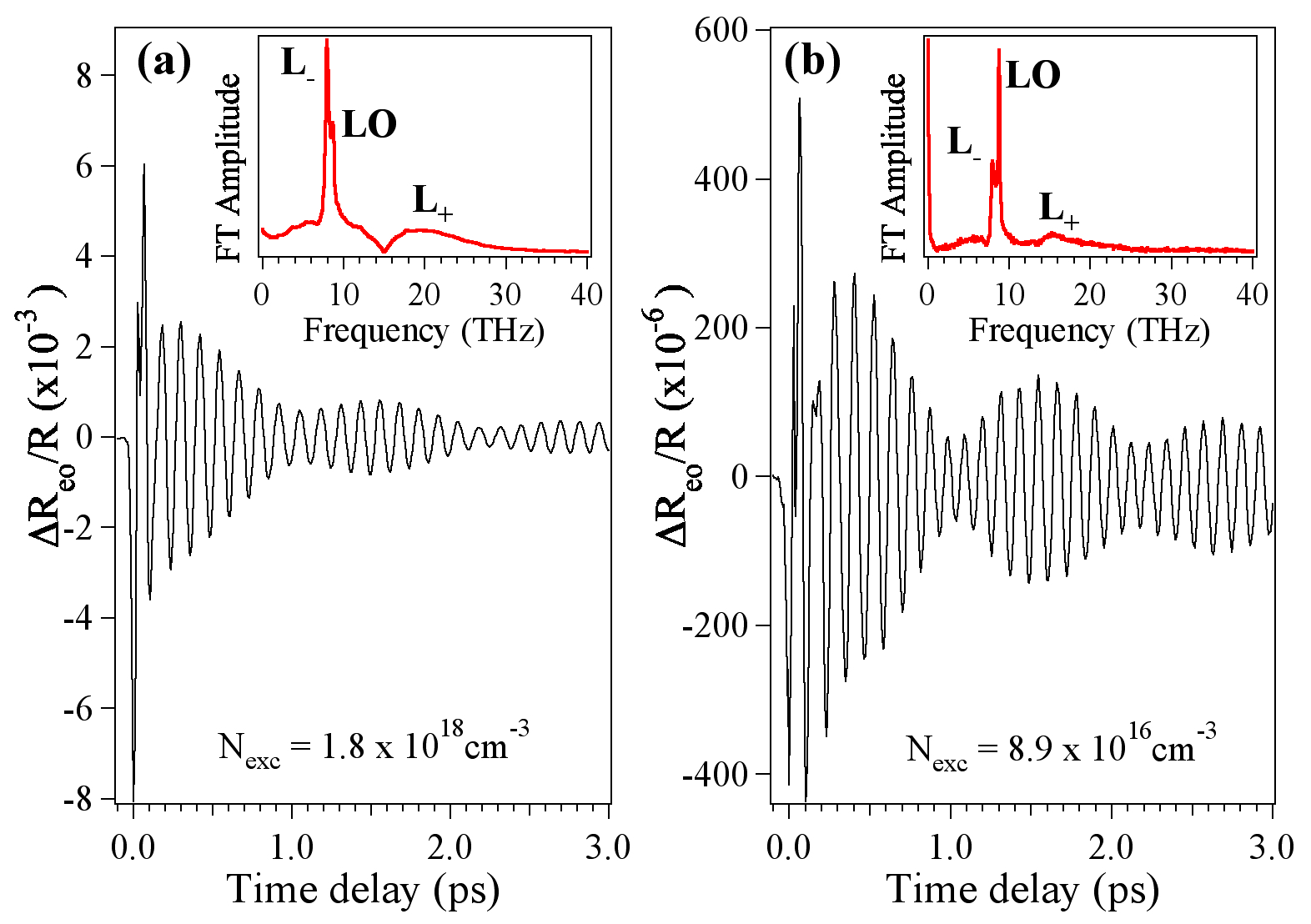
Here, the carrier
(electron) mobility was determined from the dephasing time of the
plasmon-like coherent LOPC mode (L+) in n-GaAs, which is
obtained by mapping the time-frequency dynamics of the LOPC modes by
the use of the wavelet analysis. The electron mobility extracted from
the coherent phonon spectroscopy decreases with increasing the
photo-doping levels, indicating the suppression of the mobility by
enhanced electron-hole scattering. The availability of this technique
will spread over the polar semiconductors, such as SiC, GaN, under the
condition that the photo-doping level assure that the LOPC mode is
plasmon-like.
|
|
 |